

Lithography Process: 10 Steps Of Making Photo Etching Printing
Lithography (optical exposure) refers to the process of irradiating light with a specific wavelength to transfer the graphics on the mask to the photoresist. Optical exposure is a complex physical and chemical process, which has the characteristics of large area, good repeatability, easy operation, and low cost. It is the core step of the semiconductor device and large-scale integrated circuit manufacturing. Here, we focused on the 10 steps of the photo etching printing process.
What Is Lithography (Photo Etching) Process?
1. Substrate pre-treatment
① Remove surface contaminants (particles, organics, process residues, movable ions) and water vapor;
② Pre baking to 100 ~ 200 ℃ can help to enhance the adhesion between photoresist and substrate;
③ For hydrophilic substrates (such as SiO2, glass, precious metal film, GaAs, etc.), the use of adhesion enhancers (such as AR 300-80 or HMDS) to increase the adhesion between the substrate and photoresist is called adhesion enhancement or adhesion aid.
Attachment principle of AR 300-80 new:
When ar 300-80 new (4000rpm) is spin-coated on a substrate (such as SiO2 or sin) and pre-baked at 60 ℃ (hot plate for 2min; oven for 25min), a 15nm thick diphenyl dihydroxy silane film can be obtained. The original functional groups (sio2-oh or sin-n) on the substrate will be replaced by a thin diphenyl dihydroxy silane link layer. When the photoresist is spin-coated, this thin layer of diphenyl silane will quickly dissolve in the photoresist solvent, and the diphenyl silane dissolved in the photoresist will not affect the subsequent exposure and development process. Of course, organic solvents (such as acetone, ethanol, and anisole…) can also be used to remove it, but its hydrophobic functional groups remain on the substrate surface. If it is necessary to restore the hydrophilic properties of the substrate, it can be realized by using strong alkali or plasma etching process.
2. Coating
① Gluing method: spin coating and spray coating;
② Before gluing, the substrate needs to be cooled to room temperature, and the photoresist also needs to be opened at room temperature (the supercooled photoresist just taken out of the refrigerator will condense the water vapor in the air);
③ The bubbles in the photoresist should be used after escaping by standing. When taking the photoresist with a dropper, the action should be gentle to avoid bringing in bubbles;
④ With the frequent opening of the photoresist, the solvent volatilizes, and the thickness of the photoresist will increase accordingly;
⑤ Multiple spin coating can obtain a thicker film, but the coated photoresist layer needs to be baked and cooled before coating a new adhesive layer, and the uniformity of multiple spin coating will become worse.
Influencing factors of gluing uniformity:
① Cleanliness, roughness and the hydrophobic property of substrate;
② Acceleration from low speed to high speed during spin coating;
③ Photoresist coverage before high-speed stage;
④ Spin coating time: generally, it takes a long time for thick glue, but it is unfavorable to the uniformity if the spin coating time of thin glue is too long;
3. Soft bake
① Pre drying purpose: remove the solvent in the photoresist, enhance the adhesion, release the internal stress of the photoresist film and prevent the photoresist from polluting the equipment;
② Common baking methods: hot plate, short baking time, but easy to be affected by the external environment, oven, long baking time, not suitable for thick glue baking;
③ Under drying will easily lead to residual solvent affecting the exposure and development process, and over-drying will reduce the activity of photosensitive components in photoresist;
④ For the application of substrate sensitive to temperature, the pre-baking temperature can be carried out at a lower temperature (< 60 ℃), but the baking time needs to be extended appropriately;
⑤ After baking, it needs to be cooled to room temperature before subsequent processes, especially thick glue. Before exposure, it needs to wait for a period of time to realize the reabsorption process to ensure the development speed and high contrast.
4. Exposure
① Mask alignment exposure: the mask plate is required to obtain graphics. The mask plate graphics and photoresist graphics are 1:1, contact and proximity, and the light source is usually UV light source;
② Step projection exposure: the mask plate is required to obtain the graphics. There is a projection system between the mask plate and the photoresist to expose the graphics on the photoresist according to a certain proportion;
③ Laser direct writing: use the laser beam to scan according to the preset path to obtain the graphics. Usually, DMD technology is used to realize the laser spot control to obtain the graphics without a mask.
④ Electron beams direct writing: the photoresist is exposed by using the electron beam as the light source. The exposure process uses loss or gridline scanning to obtain the pattern without a mask. It is usually divided into Gaussian beam and deformation beam.
In the exposure process, we need to control the exposure dose and obtain the corresponding reference dose according to the type of photoresist and technical data. The best exposure dose is obtained through experiments. Note that the acceleration voltage will also affect the exposure dose.
When the substrate material with poor conductivity is exposed to the electron beam, it is necessary to improve the conductivity by introducing a conductive polymer or conductive film to avoid the defects caused by the charging effect.
5. Post exposure bake-PEB
The process of baking the photoresist film after exposure. In other words, when the photoresist is not softened, the temperature of PEB can be higher than that of the photoresist film. This process step is not necessary and needs to be carried out in the following cases:
① Chemical amplification glue: the light reaction starts during the exposure period and is completed in the post-baking link. The process of “chemical amplification” takes place under the catalysis of reaction products after exposure and is completed in baking. This allows a thicker photoresist to be exposed with a lower exposure dose, and the development speed is fast;
② Pattern reversal glue and cross-linked negative glue: under the reversal process, the pattern reversal glue needs to be post-baked after exposure to realize the reversal of the pattern, so as to make the exposed area flow down after development. Crosslinked negative glue also needs to be crosslinked in the post baking link;
③ In the exposure application of a monochromatic light source on high reflectivity substrate, due to the reflection of the interface, interference will be formed in the photoresist. This interference will lead to the formation of wave stripe structure on the photoresist sidewall during development, that is, the standing wave effect. The post-baking after exposure contributes to the diffusion of photoreaction products, so the photoresist structure in the subsequent development process has steeper and smoother sidewalls.
6. Development
In the process of development, the positive glue film structure is formed by dissolving the exposed area, while the negative glue development removes the unexposed area. For repeatable results, the temperature range is 21-23 ℃, and the error is ± 0.5 °. There are three common development methods: immersion, spray, and puddle.
The common developer of UV photoresist is an alkaline aqueous solution, which can be divided into two categories: alkaline developer with metal ions and TMAH-based developer without metal ions. The developer of electron beam photoresist has a large amount of organic solvent and a TMAH-based developer. Generally, the selection of developing solution needs to be based on its own photoresist type (generally recommended developing solution), sample (such as substrate material), process (metal ion control requirements for the subsequent process), etc.
The influencing factors of development mainly include developer, development mode, and temperature. After the same photoresist developer is diluted, the development speed decreases, the contrast increases, and the development mode determine whether the photoresist has sufficient contact with the fresh developer, high temperature, and fast development speed.
7. Stopping
Fix and terminate the development process. UV photoresist is often washed with water because water-soluble alkali is commonly used as the developer; Electron beam adhesives often use organic solvents as developing solution, so a special fixing solution is needed for fixing.
It should be noted that the photoresist structure with a high aspect ratio obtained by electron beam exposure is easy to collapse under the action of surface tension due to its weak strength.
In the lift-off process, special attention should also be paid to the treatment of primer after development.
8. Hard bake
The hard film is to make the adhesive film more firmly adhere to the wafer surface by heating and baking and can increase the etching resistance of the adhesive layer. The hard film is not a necessary process. If the subsequent process is an etching process, it is recommended to carry out the hard film to improve the stability of the photoresist. If the subsequent process is a lift-off process, it is generally not recommended to carry out a hard film process, because the stability of the photoresist is improved after the hard film, which is not conducive to stripping.
In addition, we must pay attention to the temperature of the hard film. The too high temperature will deform, melt, and even disappear the photoresist structure.
Of course, we can also use this high-temperature treatment to obtain some special applications. This process is called reflow.
9. Pattern transfer
① Liftoff: it is necessary to pay attention to the relationship between the thickness of the photoresist and the thickness of metal, so as to obtain the undercut structure as much as possible. If necessary, the double-layer glue process can be used. Note that the developed primer may affect the device. The evaporation coating method needs to be selected, and pay attention to the thermal effect of thicker metal coating;
② Etching process: for dry etching, select the photoresist with good etching resistance (relative), calculate the required photoresist thickness, and pay attention to the temperature in the etching process. After etching, due to the denaturation of the photoresist, the wet method cannot complete the degumming. It is recommended to use the degumming machine. Wet etching requires the selection of adhesive with good adhesion and addiction treatment;
③ Liga: similar to wet etching, glue with good adhesion to the substrate needs to be selected to prevent glue bleaching in the liquid;
④ Ion implantation: a certain thickness of glue with good temperature resistance and mechanical stability needs to be selected. High dose ion implantation will lead to lithography denaturation, which needs to be removed by a degumming machine.
10. Remove
After the pattern is transferred, the photoresist is no longer needed, so it needs to be removed. There are usually two methods of degumming: the wet method and the dry method. The wet process is to dissolve or corrode the photoresist by using an organic solvent or solution with a corrosive effect on the photoresist, so as to achieve the purpose of degumming. Here, the selection of degumming solution needs to follow the premise of reacting with the substrate or not damaging the substrate. Dry degumming is to use of oxygen plasma to ashing photoresist, so as to achieve the purpose of degumming. For the selection of the degumming method, it is generally recommended to give priority to wet degumming, because wet degumming is simpler. If wet degumming cannot be removed, dry degumming shall be considered. It should be noted that oxygen plasma may be used in the process of dry degumming, which may oxidize the sample

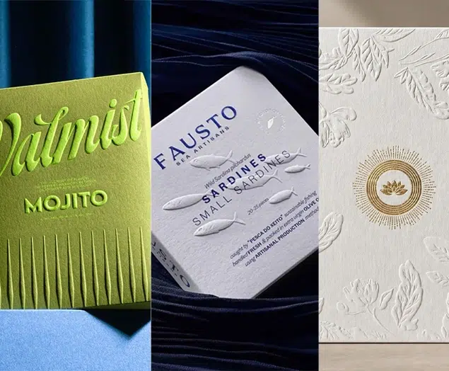
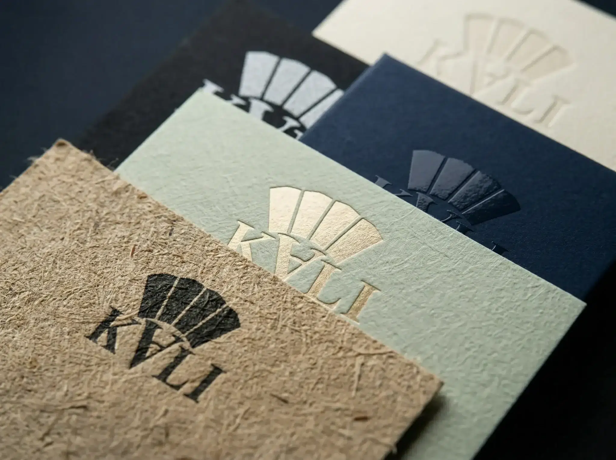
Top 10 Creative Cosmetic Packaging Design Ideas & illustrations 2023 | Luxury-Paper-Box.Com

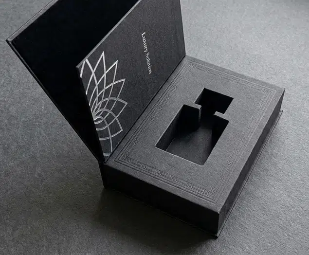
How the Right Perfume Packaging Sells the Scent

5 Eyewear Packaging Trends Shaping 2026